

For hardware startup engineers, rapid PCBA (Printed Circuit Board Assembly) prototyping is crucial in product development. While professional assembly services are available, DIY assembly during the prototype phase not only reduces costs but also deepens your understanding of circuit design and accelerates iteration cycles. This comprehensive guide walks you through the complete process—from design files to finished assembly—with clear, actionable steps and practical tips to help you avoid common mistakes.
Step 1: Generate Gerber Files and BOM
1.1 Complete PCB Design
Using EDA software such as Altium Designer, KiCad, or Eagle, finalize your schematic and PCB layout:
Pad Design: Ensure pad sizes match component packages—neither too large nor too small
Solder Mask Openings: Verify that pads requiring soldering aren't covered by solder mask
Silkscreen Markings: Include component designators (R1, C2, etc.) and polarity indicators (diode bands, capacitor "+" symbols) to aid manual placement
1.2 Export Gerber Files
Gerber files are the industry standard for PCB fabrication. Export the following layers:
Top/Bottom Copper (.GTL/.GBL)
Top/Bottom Solder Mask (.GTS/.GBS)
Top/Bottom Silkscreen (.GTO/.GBO)
Drill Files (.TXT or .DRL)
Board Outline (.GML/.GKO)
Pro Tip: Always verify exported files using free Gerber viewers like Gerbv or CAM350. Check that all layers align correctly, especially pads versus solder mask openings.
1.3 Generate BOM
Your Bill of Materials should include for each component: designator, part number, specifications, package, quantity, and recommended suppliers (DigiKey, Mouser, LCSC). Excel or CSV format works best for procurement filtering.
Stp 2: Order PCB Samples and Components
2.1 Select PCB Fabrication Service
Recommended Manufacturers: JLCPCB, PCBway, ZMS. Simply upload your Gerber files and select:
Material: Standard FR-4 works for most prototypes
Thickness: 1.6mm typical
Surface Finish: HASL (economical) or ENIG (better for fine-pitch)
Turnaround: 3-5 days standard, expedited options available
For prototypes, order 5-10 boards—cost remains minimal while providing spares.
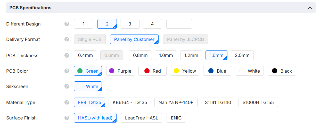
This is for reference some of the selection when ordering a customize PCB from JLC, there will be more specs and options needs to be selected before ordering. If this step is too complicated for you to understand and worrying selected wrong specs, feel free to contact Zero Mistake Solutions for fast quote and we will help with choosing the suitable specs for your PCB, compared with JLC and PCBway, ZMS will help with panalize the PCB for you in the best material usage ratio and send EQ for double confirm before production.
2.2 Component Sourcing
Purchase components from reputable distributors such as Zero Mistake Solutions based on your BOM:
Passive Components: Resistors, capacitors, inductors—LCSC offers competitive pricing for small quantities
Critical ICs/Sensitive Parts: Source from authorized distributors like DigiKey, Mouser, or Arrow to ensure authenticity
Verification: Double-check packages match your PCB footprint, especially pin spacing and orientation
Storage: Organize components by value/package and protect from moisture and ESD. For moisture-sensitive devices (MSL), follow handling guidelines from sealed packaging.
Step 3: Order Stencil Based on Gerber Files
3.1 Purpose of Stencil
Stencils precisely apply solder paste to PCB pads. For DIY assembly, laser-cut stainless steel stencils are recommended:
Thickness: 0.1mm-0.15mm typical—choose 0.1mm for fine-pitch components (0.5mm QFP)
Size: Usually larger than PCB (e.g., 400mm×300mm) for easy handling
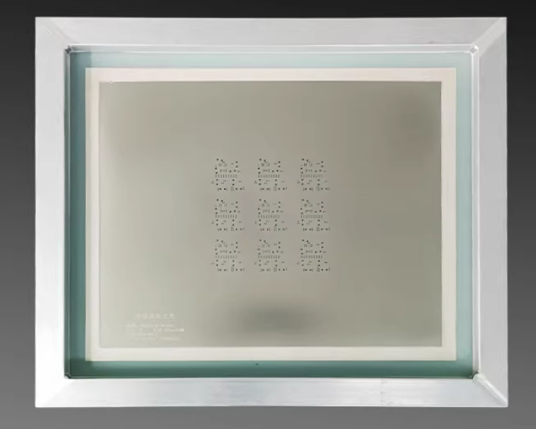
3.2 Ordering Your Stencil
Provide your Gerber files, specifically the Top Solder Mask layer (.GTS) or Top Copper layer (.GTL)—manufacturers create apertures based on pad locations
Most PCB fabricators offer stencil service—order simultaneously to save shipping
Cost-Effective Option: Frameless stencils work well for manual assembly
Alternative: Manual solder paste dispensing with syringes works but lacks precision for fine-pitch components.
Step 4: Purchase and Prepare Solder Paste
4.1 Solder Paste Selection
Type: Lead-free (SAC305) is environmentally friendly with ~217°C melting point; leaded (Sn63/Pb37) melts at ~183°C, offering easier reflow—both acceptable for prototypes
Storage: Refrigerate at 0-10°C; allow 2-4 hours to reach room temperature before use—never heat to thaw
Quality: Choose reputable brands like Kester, Alpha, or Indium
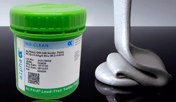
In Zero Mistake Solutions, we pay close attention to soldering quality, so we choose well-known solder paste brands such as Alpha and Senju to ensure the stability of soldering quality and make sure totally Lead-free.
4.2 Proper Mixing
Solder paste separates during storage—thorough mixing is essential:
Manual Method: Use a clean spatula to stir paste in its container for 1-2 minutes until uniform, no lumps or separation
Mechanical Mixer: Follow manufacturer instructions if available
Rest Period: Let paste sit for several minutes after mixing to allow bubbles to escape
Step 5: Align Stencil and Apply Solder Paste
5.1 Required Tools
Stencil
PCB
Alignment fixture or tape
Squeegee (metal or polyurethane with straight edge)
5.2 Stencil Alignment
Secure PCB on flat work surface using fixture or tape to prevent movement
Position stencil over PCB, aligning apertures precisely with pads
Critical Step: Use alignment pins if your PCB has tooling holes, or temporarily tape one corner and verify alignment under magnification
Ensure stencil contacts PCB firmly with no gaps
5.3 Paste Application
Place solder paste bead at one end of stencil
Hold squeegee at 45-60° angle
Apply steady pressure while moving squeegee across stencil in one smooth motion
Lift Carefully: Remove stencil vertically—do not drag sideways, which can cause paste smearing or bridging
Inspect results: All pads should have consistent paste coverage without bridges or insufficient paste
Troubleshooting: Clean PCB with alcohol and reprint if defects appear. Work in small batches—paste degrades when exposed to air.
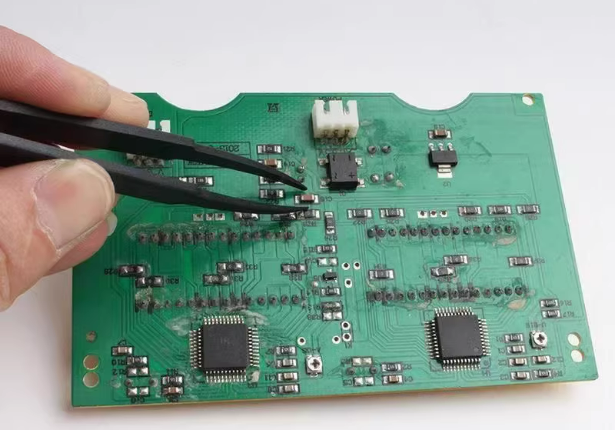
Step 6: Manual Component Placement
6.1 Essential Tools
Precision tweezers (straight and curved tips)
Vacuum pick-up tool (ideal for ICs)
Magnifying lamp or stereo microscope
ESD wrist strap (protect sensitive components)
6.2 Placement Process
Start Small: Place resistors and capacitors first—larger components later won't obstruct access
Align with Pads: Using tweezers, position component over paste-covered pads; gently set in place
For ICs: Verify all pins align with pads; use tweezers for fine adjustments
Polarity Check:
Diodes: Cathode marked with band (match PCB silkscreen)
Electrolytic Capacitors: Longer lead is positive; capacitor body shows "-" marking for negative
ICs: Pin 1 indicator (dot, notch, or chamfer) must match PCB marking
Secure Placement: Lightly press components into paste using tweezers—avoid sliding
Quality Check: After placing each few components, verify position and orientation under magnification. For fine-pitch ICs, microscope inspection is essential.
Step 7: Reflow Soldering
Choose method based on available equipment:
7.1 Reflow Oven (Recommended)
Temperature Profile: Follow solder paste datasheet—typically:
Preheat: 150-180°C for 60-120 seconds
Soak: 180-200°C for 60-120 seconds
Reflow: Peak 235-245°C (lead-free) or 210-220°C (leaded) for 30-60 seconds
Cooling: Gradual, natural cooling
Place assembled PCB in oven, run profile, inspect after cooling
7.2 Hot Air Rework Station
Ideal for small batches or rework:
Preheat PCB (hot plate or low-temperature hot air to ~100°C)
Direct hot air nozzle at component, moving in circular pattern
Heat until paste melts and forms shiny joints
Protect adjacent components with heat-resistant tape

7.3 Hot Plate Method
Place PCB on programmable hot plate
Gradually increase temperature through solder melting point
Remove once all joints reflow; allow natural cooling
Suitable for single-sided assemblies; ensure even heating

Critical Considerations:
Avoid overheating—damages components and PCB
Never quench—allow gradual cooling
Ensure good ventilation (solder fumes are hazardous)
Step 8: Inspection and Rework
8.1 Visual Inspection
Examine all joints under magnification:
Smooth, shiny appearance indicates good wetting
Check for bridges (solder connecting adjacent pins)
Verify no insufficient solder or disturbed joints
Confirm all polarities correct
8.2 Electrical Testing
Measure power rails for shorts before applying power
Perform functional testing according to design specifications
8.3 Rework Techniques
Solder Bridges: Remove with desoldering braid and flux, then reflow if necessary
Insufficient Solder: Apply flux and touch up with soldering iron or hot air
Missing Components: Add component and reflow affected area
Tombstoning: Reheat both pads equally while gently pressing component
Conclusion
By following these steps, you can successfully assemble professional-quality PCBA prototypes in your own workspace—transforming design files into functional hardware in days rather than weeks. DIY assembly accelerates design validation, builds invaluable hands-on experience, and provides flexibility during early-stage development. As your product matures toward production, professional assembly services become appropriate, but mastering DIY PCBA skills gives hardware entrepreneurs confidence and agility throughout the development journey. Happy building!
Zero Mistake Solutions is offering prototyping to mass production services for our clients, if you need help in any parts or any progress in your project, feel free to contact us for more discussion.